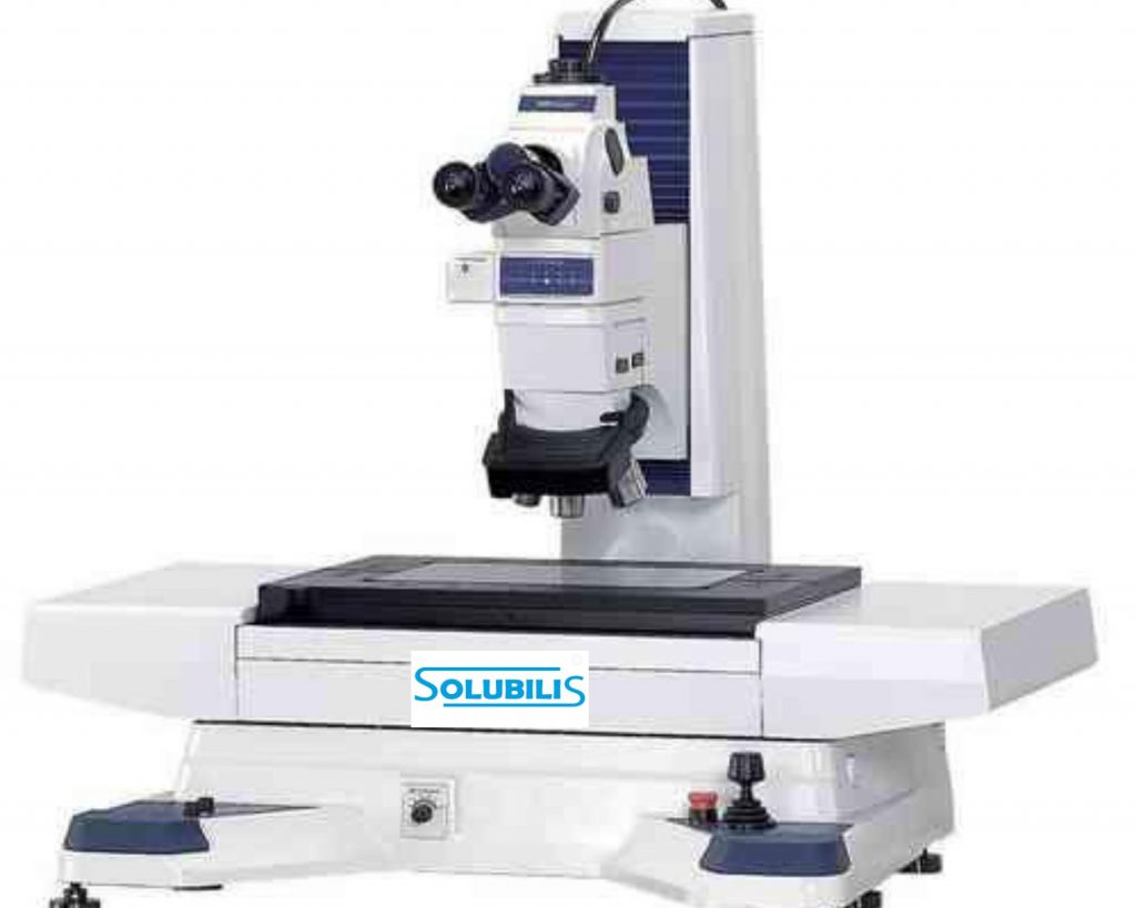
What is Lithography metrology?
TALK TO EXPERTS
Lithography is a process where a pattern from a photomask is moved to the outer layer of the wafer. During the lithography process, the wafer gets presented to bright laser shaft, in which the bright laser bar goes through photomask layer without a pattern and is lighted onto photoresist on a wafer. Metrology is fundamental for control, advance, and guarantee the best return in semiconductor producing measures. The lithography metrology equipment has made development roads in the semiconductor business because of its high reception rates worldwide.
As per the lithography metrology equipment market analysis, lithography metrology hardware is utilized for different factors like basic measurement estimation, imaging of wafer designs utilizing photoresist, deformity examination, design measure advancement, and material screening. A significant limitation, which influences the lithography metrology market is quick headway of designing innovation, which builds its general expense.
The key factors that drive the development of the lithography metrology hardware industry incorporates appeal for scaled down electronic gadgets, expansion in patterns toward Internet of Things, and advancement in wafer size patterns. Notwithstanding, high functional and support cost of metrology equipment and metrology challenges winning for complex IC gadgets hampers the market development partially. Besides, expansion in headways in cutting edge metrology procedures offers worthwhile freedoms for the lithography metrology equipment market development internationally.
Segmentation
The lithography metrology equipment market size is classified based on innovation, item, application, and district. Contingent upon innovation, the market is grouped into basic measurement examining electron magnifying instrument (CD-SEM), optical basic measurement metrology (OCD), overlay control, and others. Side-effect, the market is dissected across substance control equipment, gas control hardware, and others. By application, the market involves quality control and examination, figuring out, programmatic experience, and others. In view of area, the market is contemplated across North America, Europe, Asia-Pacific, and LAMEA, alongside its conspicuous nations.
These central participants embrace a few methodologies, for pattern, new item dispatch and advancement, procurement, organization, cooperation, and business extension to build the lithography metrology equipment portion of the overall industry during the estimate time frame.
Top Impacting factors
The components like appeal for scaled down electronic gadgets, expansion in patterns toward Internet of Things (IoT), development in the semiconductor business, issues with respect to metrology challenges for complex ICs, and arising patterns toward expansion in interest in wafer creation hardware and materials are relied upon to fundamentally influence the development of the worldwide lithography metrology equipment market size. These components are expected to one or the other drive or hamper the lithography metrology equipment development.
High demand for electronic devises
Scaled down electronic gadgets are encountering development in the semiconductor business because of ascend popular for elite hardware. Moreover, expansion sought after for upgraded customer gadgets fills the prerequisite of adaptable and minimal coordinated circuits. Additionally, ascend in improvements of advancements like RFID, MEMS gadgets, and other force gadgets help the interest for flimsy wafers. For pattern, wafer backgrinding measure is used to decrease the thickness of wafers from 750 μm to around 75-50 μm. Slim wafers help in decreasing the thickness of bundles, particularly for cell phones, handheld gadgets, and conservative electronic items. For these arising applications in innovation that utilization exceptionally dainty and super meager kick the bucket, provoke colossal interest for scaled down electronic gadgets and further aid the development of lithography metrology hardware portion of the overall industry internationally.
Metrology challenges
One of the main considerations that impedes the development of the lithography metrology gear market is design intricacy of coordinated circuits in semiconductor wafers. By and large, chip and microcontrollers contain numerous semiconductors and extensive copper lines in the design of coordinated circuits and semiconductor wafers. What’s more, semiconductors ought to be exceptionally dependable, which includes different designs and examples to improve its functional productivity.
The design chain of ICs and semiconductor wafers utilized in industry verticals, for example, car, medical services, and aviation and guard are more perplexing than ICs utilized in gadgets, cell phones, and others. This makes the design of exceptionally solid and upgraded ICs a troublesome undertaking for the metrology process and goes about as a significant obstruction for the lithography metrology hardware market.
Increase in investment
There is an increment in pattern toward developing interests in wafer manufacture gear and materials, which gives worthwhile development freedoms to the semiconductor business. States of different creating areas, for example, South Korea, Taiwan, and China are setting up guidelines to inspire the semiconductor business by taking on methodologies like business development, securing, and different item dispatches.
For example, Shanghai Jita Semiconductor, an auxiliary of Huada Semiconductor and China Electronics Corporation (CEC), declared to fabricate both 200 mm and 300 mm semiconductor fabs for simple and force semiconductors in Shanghai from 2019.
The consolidated fab venture will add up to $5.18 billion. Furthermore, Hamamatsu, a semiconductor organization situated in Japan declared that it is building another office speculation of 2.8 billion Yen (US$25 million) to help the semiconductor limit in the country. This load of speculations drive the interest for wafers, Ic’s, and chips markets, which thus makes worthwhile lithography metrology gear market opportunity for wafer creation cycle and lithography metrology.
Benefits of Lithography metrology
- This review incorporates the insightful portrayal of the worldwide lithography metrology hardware market figure alongside the latest things and future assessments to decide the approaching speculation pockets.
- The report presents data with respect to the key drivers, restrictions, and openings in the lithography metrology hardware market.
- The lithography metrology gear market development is quantitatively examined from 2019 to 2026 to feature the monetary skill of the business.
- Porter’s five powers investigation shows the strength of the purchasers and providers in the business.
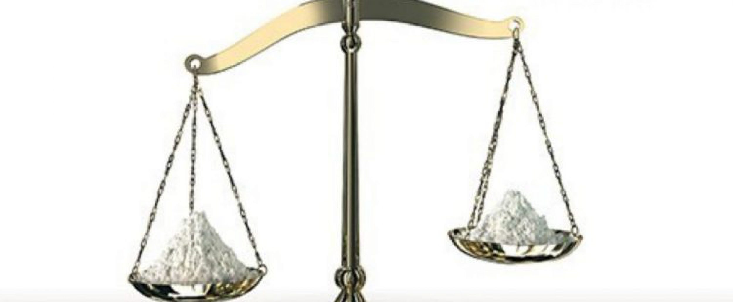
Legal metrology
Legal metrology includes the organization of estimating instruments, application for units of estimation, and testing strategies which are regularly settled in one or the other enactment or recorded norms. The object is to give exact and dependable estimations to trade, wellbeing, security, and the climate.
Organization of legal metrology exercises are performed by or with oversight from states to give the suitable degree of dependability and believability. Legal Metrology is upheld by the International Organization of Legal Metrology (OIML), whose statement of purpose is to:
- empower economies to set up viable legal metrology foundations that are commonly viable and globally perceived, for all spaces for which legislatures assume liability,
- for example, those which work with exchange, set up shared certainty and fit the degree of customer security around the world.